Tiny displacements, giant changes in optical properties
Materials scientists led by Rohan Mishra and Jayakanth Ravichandran reveal pathway for designing optical materials with specialized properties

Watch out, Marie Kondo. While we usually think of disorder as a bad thing, a team of materials science researchers led by Rohan Mishra, from Washington University in St. Louis, and Jayakanth Ravichandran, from the University of Southern California, have revealed that – when it comes to certain crystals – a little structural disorder might have big impacts on useful optical properties.
In a study published online March 23 in Advanced Materials, first authors Boyang Zhao, a USC graduate student in materials science working with Ravichandran, and Guodong Ren, a graduate student working with Mishra in WashU’s Institute of Materials Science and Engineering, described a new pathway to obtain novel optical and electronic properties from structural disorder. They found that tiny displacements of just a few picometers – that’s 100,000 times smaller than the thickness of a sheet of paper – in the atomic structure of a crystal could have minimal impacts on optical properties in one direction but produce giant functional enhancements when viewed from another angle.
In this case, the refractive index of the material, or how much light bends or deviates from its original path when is passes through, changed dramatically with atomic disorder.
Such functional enhancements could have practical applications in imaging, remote sensing and even medicine. By controlling the degree of atomic disorder to achieve desired optical properties, the researchers anticipate developing crystals that enable advanced infrared imaging in low light conditions, for example, improving the performance of autonomous vehicles driving at night or medical imaging devices.
“We’ve been working on semiconductor materials for years, gradually moving down the periodic table, looking for materials that behave well but also do interesting or unexpected things,” said Ravichandran, the Philip and Cayley MacDonald Endowed Early Career Chair and associate professor in the Viterbi School of Engineering at USC. “When we started looking at ways to get more tunability – to craft materials ideally suited for specific applications – we found that properties varied dramatically when measured from different directions.”
When materials have different properties or behavior when measured or observed from different directions, that’s known as anisotropy. Anisotropic materials have different characteristics depending on how you look at them, and that can make a huge impact on features including light transmission, mechanical behavior, and other physical or electrical properties critical to the functioning of everyday devices like cameras.
The material the team studied, barium titanium sulfide (BaTiS3), a hexagonal crystal, was already known to have large optical anisotropy, but scientists couldn’t figure out why. It took years of back-and-forth collaboration between teams at WashU, USC and various national labs, but eventually the team cracked the case.
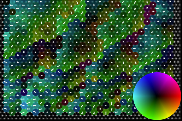
“We were seeing big discrepancies between theory and experiment – shining a light on the material at different angles was making a huge difference in optical properties for reasons that weren’t clear,” said Mishra, associate professor of mechanical engineering & materials science in the McKelvey School of Engineering at WashU. “The key turned out to be structural instabilities that result in certain atoms, in this case the Ti atoms, to displace away from more symmetric positions in a disordered manner. Small anisotropic displacements showed up in high-resolution synchrotron experiments, then we knew to look closer at the atomic structure using an electron microscope.”
“Picometer-scale displacements are so tiny that you’ll only find them if you’re specifically looking for them,” Ravichandran added.
That level of fine detail usually isn’t needed, even for cutting-edge materials science research, because light vibrates so quickly that it smooths over local imperfections in a material. Not this time.
Ren and Zhao had to look at every assumption and every piece of theory to figure out how to explain the mismatch between theory and experiment, Mishra and Ravichandran said, noting that solving this mystery was only possible through collaboration. Using a combination of advanced techniques including single crystal X-ray diffraction, solid-state nuclear magnetic resonance and scanning transmission electron microscopy, the researchers found evidence of anisotropic atomic displacements of the titanium atoms in BaTiS3. These incredibly tiny, picoscale displacements happen in local clusters within the material, yet they exert a profound influence on global optical properties.
“The key thing is that tiny displacements can have giant effects,” Mishra said. “We’re still exploring how factors like temperature might change this material’s optical properties, but with this study we’ve developed a deep understanding of the relationship between structural disorder and optical response. That will help as we continue discovering new materials and functionalities.”
Zhao B, Ren G, Mei H, Wu VC, Singh S, Jung GY, Chen H, Giovine R, Niu S, Thind AS, Salman J, Settineri N, Chakoumakos BC, Manley ME, Hermann RP, Lupini AR, Chi M, Hachtel JA, Simonov A, Teat SJ, Clément RJ, Kats MA, Ravichandran J,and Mishra R. Giant modulation of refractive index from picoscale atomic displacements. Advanced Materials, online March 23, 2024. DOI: https://doi.org/10.1002/adma.202311559
This work was supported by the Army Research Office (W911NF-19-1-0137 and W911NF-21-1-0327), the National Science Foundation (DMR-2122070, 2122071 and 2145797), the Air Force Office of Scientific Research (FA9550-22-1-0117), the Office of Naval Research (N00014-20-1-2297), the USC Provost New Strategic Directions for Research Award, and the U.S. Department of Energy Office of Science.


